|
The
O-lattice
theory fully accounts for the structure
of phase boundaries, too - as long as we look at two crystalline phases, of
course. It is, however still not easy to use (it is waiting for someone to turn
it into a user-friendly piece of software), and it can not answer a few
specific question about the development of
the structure whenever a phase boundary is formed. |
|
So for phase boundaries, too, it is
often more easy to think in terms of the simpler coincidence lattice - but with a grain of salt. A few special points
are: |
|
 |
In general, there will be no suitable coincidence lattice at all, because
the lattices are different and their lattice constants are incommensurable
(their quotient is an irrational number). In practice, however, we do not know
the lattice constants to an arbitrary degree of precision, and you will always
find some fitting relation. |
|
|
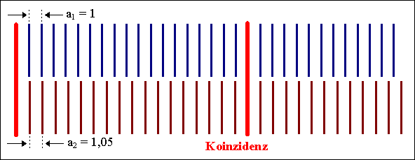
Even if there is a CSL, it is not necessarily the proper reference lattice. This
can be seen from a simple example: Two cubic crystals with lattice constants
a1 = 1 and a2 = 1,05 (i.e. a
misfit of 5%) from a phase boundary: |
|
|
|
|
|
|
|
|
|
|
We have a perfect two-dimensional
CSL structure (Σ2d = 20
would hold for 2 dimensions), |
|
|
Note that we can have situations (like even Σ numbers)
which are simply not possible for grain
boundaries, where the lattice constants are the same by definition. |
|
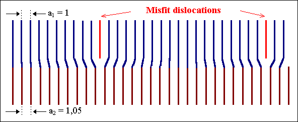
It is much more sensible to describe
this phase boundary as a Σ = 1 boundary with
superimposed phase boundary
dislocations (which we practically always will call
misfit dislocations) as shown below,
because this is usually an energetically better situation than a Σ2d = 20 (or whatever) boundary with no
dislocations. |
|
|
The misfit dislocations in this case are more or
less lattice dislocations of the crystals - but that does not mean that
DSC lattice dislocations never occur in phase boundaries! |
|
|
|
|
|
|
|
|
|
Misfit dislocations compensate for
differences in the lattice constants by concentrating the misfit in
one-dimensional regions - the dislocation lines. |
|
|
Between the dislocation lines the interface is
coherent; a phase boundary with misfit
dislocations is called semi-coherent. |
|
|
Misfit dislocations - in contrast to general
grain boundary dislocations - must have an edge
component that accounts for the lattice constant mismatch |
|
Whereas the O-lattice theory
as applied to phase boundaries allows phase boundary dislocations in general
(of which misfit dislocations are only a subset), "simple" misfit
dislocations are the dominant defects in technologically important man-made phase
boundaries. |
|
|
Misfit dislocations are not restricted to
boundaries between two chemically different types of materials. Silicon heavily
doped with, e.g., Boron, has a slightly changed lattice constant and thus
formally can be sen as a different phase. The rather ill defined interface
between a heavily doped region and an undoped region thus may and does have
misfit dislocations, an
example is given in the illustration. |
|
|
The mere existence of misfit dislocations coupled
with their usually detrimental influence on electronic properties is the reason
why many "obvious" devices do not exist at all (e.g. optoelectronic
GaAs structures integrated on a Si chip), and others have
problems. The aging of Laser diodes, e.g., may be coupled to the behavior of
misfit dislocations in the many phase boundaries of the device. |
|
|
Optoelectronics in general
practically always involves having phase boundaries, e.g. devices like Lasers,
LEDs, as well as all multi quantum well structures. A very careful
consideration of misfit and misfit dislocations is always needed and some
special
process steps are often necessary to avoid these defects. |
|
However, not every (Σ = 1) phase boundary with some misfit between the
partners contains misfit dislocations - provided one of the phases consists of
a thin layer on top of the other phase.
Only if the thickness of the thin-layer phase exceeds a critical value, misfit dislocations will be
observed. It is easy to understand why this is so: |
|
|
For thin layers, it may be energetically
more favorable to deform the layer elastically, so that a perfect match to the
substrate layer is achieved. The total elastic energy contained in the "strained layer" scales with the thickness
of the layer and the expenditure in elastic energy below a
critical thickness
for an epitaxial layer may be smaller than the energy needed to introduce
misfit dislocations. |
|
This is a situation not dealt with in
the O-lattice theory or its simple CSL version. A new theory is needed. |
|
|
|
The critical thickness for the
introduction of misfit dislocations can be obtained by equating the energy
contained in a misfit dislocation network with the elastic energy contained in
a strained layer of thickness h. |
|
|
Since the elastic energy increases directly with
h, whereas the energy contained in the dislocation network
increases only very weakly with h, the thickness for which both
energies are equal is the critical thickness hc.
Thicker layers are energetically better off with a dislocation network, thinner
layers prefer elastic distortion. |
|
|
This computation was first done by
Frank and
van der Merve
in 1963; the resulting Frank and van der Merve
formula became quite famous. |
|
Somewhat later in 1974
Matthews and
Blakeslee
reconsidered the situation and looked at the forces needed to move a few
pre-existing dislocations into the interface in order to form the misfit
dislocation network. They obtain the same formula for the critical thickness as
van der Merve (i.e. the equilibrium situation), but their treatment also allows
to consider the kinetics of the process to
some extent (i.e. how the network is formed) and is therefore widely used. |
|
|
We are looking at the situation retrospectively by studying an article of the
possibly most famous TEM and defect expert, Peter Hirsch from Oxford University, or, to be
precise, Sir Peter
as he must be called after his nobilitation by Elizabeth I, Queen of England. |
|
|
This is to show that - honorwise - a defect
expert can go just as far as a rock star (several of which have been knighted
by the queen - most famous the Beatles).
Moneywise, however, it is a completely different matter. |
|
|
We use parts of his
article printed in the Proceedings of
the 2nd International Conference on Polycrystalline Semiconductors
(Schwäbisch Hall, Germany, 1990, p. 470). Do look it up - it is part of the lecture! |
|
|
|
|
|
As you saw, great minds sometimes
make great steps and are not immune to small errors! If you didn't see that,
consider: |
|
|
How exactly do you get
eq.
1? |
|
|
Why is the strain for minimum energy calculated
in eq.
3 equal to the unrelaxed elastic strain at the point of the
introduction of dislocations? |
|
|
What is h, the thickness of the
layer, doing in an equation for the critical thickness
hc (eq. 5)? After all, the
critical thickness can not possibly depend on the thickness itself. |
|
Well, if you want to know, turn to
the annotated version of
Sir Peters paper. |
|
|
|
|
Still, Sir Peter got it right in
principle, and his derivation of the critical thickness is short and most
elegant. The final formula for the critical thickness
hc is |
|
|
|
|
|
| hc |
= |
b
8π · f · (1 +
ν) |
· ln |
e · hc
r0 |
|
|
|
|
|
|
|
With b = Burgers vector of the
misfit dislocations (actually only their edge component in the plane of the
interface), f = misfit parameter, i.e Δa/a, e = e = 2,7183... = base of
natural logarithms, and r0 = core radius of the
dislocations. |
|
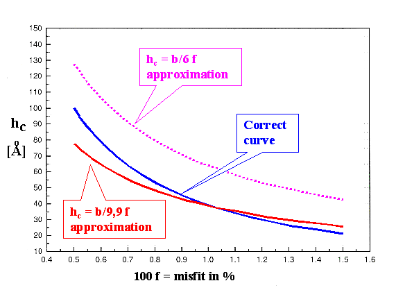
|
This transcendental equation may be roughly
approximated by |
|
|
|
|
|
|
|
|
|
|
Lets see what the
calculations tell us for real phase boundaries (for a b value of
0.376 nm (which applies to Si)). We note that misfit dislocations
are only to be expected if the layer thickness h exceeds the
critical value hc. |
|
|
|
|
|
|
|
|
|
|
|
For a misfit of 1% the critical thickness
is about 4 nm - not much at all!
|
|
This situation provides for many
technological problems, especially in semiconductor technology. It imposes
severe limits on "heterojunctions", i.e. electronic junctions between
two materials because a misfit dislocation network will invariably
"kill" your device - if not immediately, somewhat later (which is
often worse!). |
|
|
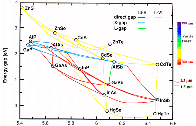
Looking at common technical semiconductors, we
realize that we have major problems in making heterojunctions: |
|
|
|
|
|
|
|
|
|
|
|
Misfits between two materials tends to be large
(not even considering Si with a lattice constant of a = 0,532
nm), and dislocation free interfaces do not come easy, if at all. |
|
|
A large group of researchers has been (and still
is) looking for ways to beat the critical thickness limitations. There are
many
tricks (the link contains a few), but hard work is needed just as much as
some luck and good ideas. A particularly clever recent idea known under the
heading of "compliant
substrates" is described in an advanced module. |
|
Experiments confirm the theory. Very
thin epitaxial layers of a second phase do not show dislocations in the
interface, but with increasing thickness misfit dislocations will appear. |
|
|
Considering that misfit dislocations are usually
unwanted but that they must appear with increasing layer thickness - however
not out of thin air - we ask an important question: |
|
Exactly how are misfit dislocations
produced and incorporated into the interface if the critical thickness is
reached. More to the point: How can I prevent this nucleation and migration process? |
|
|
Suffice it to say that while this question has
not been fully answered, there are many ways and tricks to keep misfit
dislocations from appearing at the earliest possible moment. |
|
|
The issue is sufficiently important in
optoelectronics to merit more discussion.
More
information to this point can be found in various modules of the
Hyperscript "Semiconductors". |
|
|
|
|
Even coherent phase boundaries can
still contain other defects besides misfit dislocations (not to mention
incoherent phase boundaries). In particular, we must expect: |
|
|
Dislocation
networks besides the misfit dislocations that compensate for small
tilt and twist components in analogy to the
small angle grain boundaries. |
|
|
Steps
associated with dislocations (so-called incoherent
steps) in analogy to the steps encountered in
grain
boundaries. |
|
|
Coherent
steps (without any dislocation character) as something new. |
|
After all, the surface of a substrate
on which we deposit a layer of a second phase will, in general, not be
atomically flat. Steps thus must
be expected to be an integral part of the phase boundary. We will examine some
examples for this in the next
subchapter. |
|
Next, it is important to realize that
semicoherent phase boundaries can have other CSL relation besides
Σ = 1, in particular Σ = 3, but other values, too. |
|
|
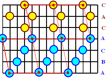
As the most important example, consider a
hexagonal lattice matched to the
{111} plane of a fcc lattice. It is
found to be in a Σ = 3 relationship, easily
seen if you compare the stacking sequences in the picture below: |
|
|
|
|
|
|
|
|
|
|
|
The ACACACA... stacking sequence of the
hexagonal lattice fits right on the ABCABCA.. stacking sequence of the
fcc lattice on a {111} plane. The Σ
= 3 relationship is clearly visible; it is indicated by red dots and
lines. |
|
|
There are of course more complex geometries - if
the CSL concept is not applicable; the O-lattice concepts has to
be used. |
|
Sorting out the various types of
possible defects is no longer an easy task. The interpretation of TEM
micrographs may become quite involved. |
|
|
Some examples will be discussed in the case
studies in the next subchapter. |
|
|
|
© H. Föll