|
In 1997, the idea came up to
accomodate the stress in a phase boundary arising from the misfit by using
existing defects some distance away from the interface which then may not be
harmful to the device. In particular, a small-angle grain boundary some 100
nm away from the phase boundary was found to do the job. |
|
 |
The concept is easy to understand on
the background of the case studies for small angle twist
boundaries discussed before. |
|
|
Lets discuss how you can make a
phase boundary free of misfit dislocations even for
misfits > 10 % and layer thicknesses of many nm. We
will do this in the form of a recipe, giving the ingredients with a brief
discussion of what they do. |
|
Lets assume we want to produce a
GaAs layer on top of a Si substrate (this is something a lot of
people would love to do! 1)).
The misfit - roughly - is 10 % so there is no chance whatsoever to
produce a misfit dislocation free interface by just depositing GaAs on
top of Si. We do it as follows: |
|
|
Bond two Si wafers together
with a (twist) misorientation of about 10o. A small angle
grain boundary will form that is identical to the one
shown before -
except that the spacing of the dislocations will be considerably smaller. |
|
|
Polish off one of the wafers until
only a layer with a thickness of a few 100 nm remains. This is not
exactly easy, but state of the art in wafer processing. |
|
Now you have a
compliant substrate. Deposit your
GaAs on top of it and be confident that you have no misfit dislocations
in the phase boundary. |
|
How does this work? On the one hand,
the details are none to clear, one the other hand, it is simple. We look at the
other hand. |
|
|
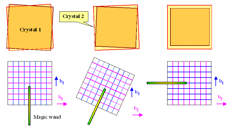
Imagine a
magic wand that you can glue to
the screw dislocation network in the small angle grain boundary. Now hold your
substrate crystal firmly in place, and rotate the
complete dislocation network by 90o. What then
happens is shown below. |
|
|
|
|
|
|
|
|
|
|
|
If you rotate the dislocation
network by 90o, you produce an edge
dislocation network. Remember that the Burgers vector is fixed; it does not depend on the
direction of the line vector - which is the
only vector you change by the rotation. |
|
|
The spacing d of the
dislocation network remained unchanged and it is now exactly the kind of
network you need to accommodate differences in lattice constants. Compare the
networks in the small
angle twist boundary in {111} Si with the
network in the phase
boundary {111}Si - (hex)NiSi2. While the networks are
identical in geometry, one consists of screw
dislocations, the other one of edge
dislocations. |
|
|
In the twist boundary, the
misorientation angle was given by (approximating sin(α) » α): |
|
|
|
|
|
|
|
|
|
|
|
For an edge dislocation network, the
misfit in lattice constants is
simply |
|
|
|
|
|
|
|
|
|
|
|
We thus can now accommodate a misfit
of |
|
|
|
|
|
|
|
|
|
|
Wow! An angle of 10o,
easily within the range of small angle grain boundaries, will have a value of
about 0,175 in angular radians and thus corresponds to a misfit of
17.5 % !!!! |
|
|
If this works, we could accommodate
huge misfits with no dislocations in the phase boundary. The prize to pay is
that we have a dense area of edge dislocations some 100 nm below the
phase boundary. But that may not be detrimental to the electronic or
optoelectronic uses you had in mind for your phase boundary. |
|
The question, of course, is: Does it work? Especially if your magical wand is at
the repair shop? The answers are: |
|
|
1. Yes - it works, at least
in principle. But much research and optimization needs most certainly to be
done before compliant substrates can be used for products. |
|
|
2. Your magic wand is
supplied by the forces acting on the dislocations as soon as you start
depositing the strained layer. These forces will try to rotate the dislocations
from screw to edge orientation. So not having a wand is not the real
problem. |
|
|
However, there is no way to rotate a
complete network as a whole. But patches of
network, separated by a third set of dislocations accommodating steps or some
small tilt component as seen in the
example, can
possibly rotate independent of each other. |
|
Finding out exactly how this can
happen (and thus how to optimize it by creating an optimized boundary
structure) will be one of the keys for success with this technique. |
|
|
This shows to demonstrate that
knowing a few things about dislocations may come in handy one day. |
|
|
So try it. See if you can figure out
how the screw dislocation network can rotate patch by patch by suitable
dislocation interactions, involving, maybe, a bunch of additional dislocations
as needed, e.g. to accommodate a small tilt component. |
|
|
|
|
|
|
© H. Föll