|
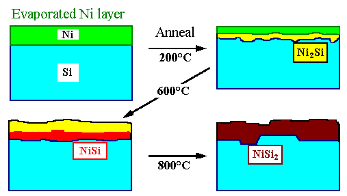
We will look in some detail on the
system Si - silicide - metal, where many phase boundaries can be
observed. The basic experiment consists of depositing a metal (here Ni)
on Si (either in a {100} or {111} orientation), and induce
some reaction by heating. |
|
 |
Three different Ni-silicides will form
consecutively: |
|
|
|
|
|
|
|
|
|
|
Altogether five different phase
boundaries may be encountered, some of which are shown in the picture above:
|
|
|
Si - Ni,
Si - Ni2Si and Ni2Si - Ni,
Si - NiSi and NiSi - Ni2Si,
Si - NiSi2, and NiSi2 - NiSi. |
|
Major findings are: |
|
|
The interface between Si and Ni
does not really exist because immediately after the (room temperature)
evaporation, a thin Ni2Si-silicide layer forms between the
Si and the Ni. |
|
|
The Ni2Si layer is
polycrystalline; the interface between Si and Ni2Si
seems to be incoherent - i.e. if there is any structure it is not observed with
"normal" TEM. |
|
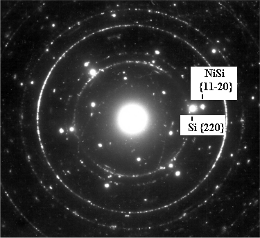
The interface between {111}
Si and NiSi is epitaxial, however, and thus semicoherent against all expectations: |
|
|
NiSi is reported to
crystallize in an orthorhombic lattice; on
{111} Si substrates, however, a hexagonal lattice is observed (which can be
cobtained from an orthorhombic lattice by slight adjustments of the lattice
parameters). |
|
|
The misfit is extremely
large (ca. 15%) and would require a distance of 0,6 nm
for b = a/2<110> misfit dislocations. Such a small
spacing is usually considered to be too small to be meaningful - epitaxial
relationships thus should not exist. The diffraction pattern, however,
indicates a clear epitaxial relationship (with a bit of polycrystallinity as
indicated by the rings): |
|
|
|
|
|
|
|
|
|
|
|
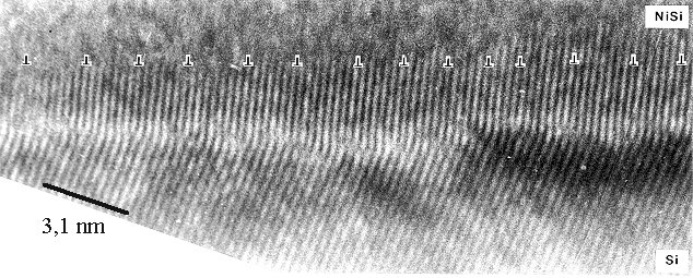
While no structure can be seen in conventional
TEM, high-resolution TEM shows pronounced misfit dislocations
relieving some of the stress at a spacing of about 1,6 nm. This is one
of the densest misfit dislocation networks ever observed. The ending lattice
planes are indicated by the edge dislocation symbol somewhat above the actual
interface plane. |
|
|
|
|
|
|
|
|
|
|
The most interesting phase is
NiSi2; it is the final product after sufficient annealing at
800 °C. |
|
|
NiSi2 crystallizes in the cubic
CaF2
- structure with a lattice constant that is only 0,3% smaller than
that of Si. |
|
|
We thus can expect an epitaxial
relationship with a misfit dislocation network at a
spacing |
|
|
|
|
|
| p |
= b · |
b
(ae – am)/am |
= |
b
0,003 |
|
|
|
|
|
|
|
With aSi = 0,54 nm and
b = a/2<110> = 0,382 nm we would expect a network
with a spacing of about 130 nm. |
|
|
What we see for an interface on a {111}
plane looks like this: |
|
|
|
|
|
|
|
|
|
|
|
This looks rather interesting. We seem to have a
simple hexagonal network of dislocations, but we see some additional features:
"Blackish" areas and an island with rather coarser structures
embedded in a sea of something with a possible hexagonal symmetry. |
|
The reasons for these complications
are two peculiarities of this interface, which can also be found in similar
systems; in particular in the Si - CoSi2 interface. |
|
|
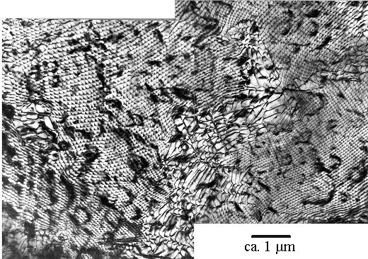
First, it
"likes" to be on {111}-planes. This leads to heavy facetting
if the Ni layer is deposited on a Si {100} plane, but also to
some facetting on {111}. This can be seen best in cross-section;
an example is given in the
illustration. We must expect that the accommodation of steps will introduce
irregularities into the network. |
|
|
Second, the
interface is mostly not in a Σ = 1 relation, i.e. with a direct continuation of the
lattices, but in a Σ = 3 relation. This means
that the NiSi2 is twinned
with respect to the substrate. An
overview picture is shown in
the link. This somewhat surprising result can be obtained from a careful
contrast analysis of the network with micrographs taken at higher
magnifications. The network then looks like this: |
|
|
|
|
|
|
|
|
|
|
|
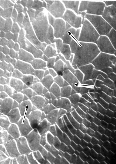
Shown is one of the "islands" in a sea
of regular hexagonal dislocations. Its structure looks
somewhat
familiar: The arrows point to extended stacking fault knots as in the case
of the small angle twist grain boundary on {111} in Si. |
|
|
But in contrast to the network in the small angle
twist boundary, all dislocations now are edge
dislocations; as expected for misfit dislocations. The distance is
also what would be expected for a almost fully relaxed layer of
NiSi2. |
|
The question is, of course, why this
mix of Σ = 1 and Σ = 3 relations? As in the case of the low angle twist
boundary encountered before, nobody knows
for sure. Obviously, the energy balance is rather similar for the two
cases. |
|
|
Very similar interfaces have been observed in the
case of Si - CoSi2 interfaces, which, except for a slightly
larger misfit, have essentially the same geometry. |
|
Despite the structural similarity to
the small angle grain boundaries, the phase boundaries add new features and
open questions. To get more insights, we will now discuss the case of the
interface between (cubic) Si and (hex.) Pd2Si. |
© H. Föll