|
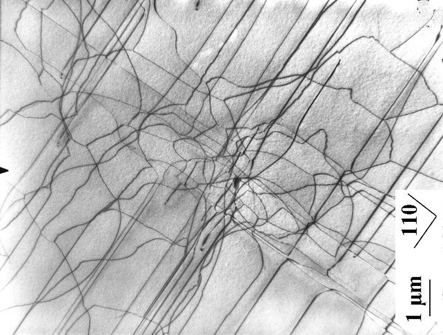
The TEM micrograph shows a
loose network of dislocations between "regular" and heavily
B-doped Silicon. The expected square network has not yet fully
developed. Many dislocations are "on their way" from the surface to
their proper place in the interface. |
|
 |
The geometry is also not too well defined, because there is no
abrupt change of lattice constants as in the case of phase boundaries between
chemically different phases. The lattice constant changes continuously
following the B-concentration which obeys some diffusion profile. |
|
|
|
|
|
|
|
|
|
|
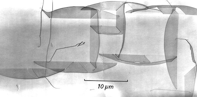
On occasions, a stacking fault
network instead of a dislocation network is observed as shown below. The
reasons for this unclear. Stacking faults of this gigantic size should be
totally unstable and would be expected to unfault. |
|
|
|
|
|
|
|
|
© H. Föll