|
In what follows a few examples for
imaging dislocations with TEM are shown. Where possible, examples have
been selected that have been used before (e.g. in the context of dislocation
loop formations) or will be used later (e.g. in the context of defects in
boundaries). |
|
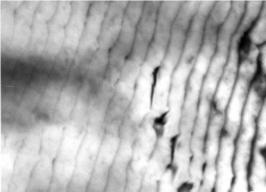
The first example demonstrates the
contrast of dislocations as a function of the excitation error |
|
|
|
|
|
|
|
|
|
 |
The specimen was bent a little; so the excitation
error changes from left to right. On the left hand side, the excitation error
is relatively large; on the right hand side it is small. The contrast on the
left is weak, but the resolution is good; on the right hand side the
dislocation appears a as strong, but blurred black line. |
|
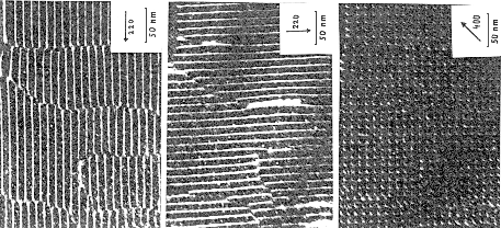
The second example demonstrates the
contrast disappearance for g · b = 0. |
|
|
Shown is a network of pure screw dislocations in
Si which we will encounter again in the context of grain
boundaries. |
|
|
|
|
|
|
|
|
Only one set of dislocations shows up
in the dark field conditions employed for the g = {220} type of
diffraction vector which is parallel to one Burgers vector and perpendicular to
the other one. With a g = {400} diffraction vector both sets of
dislocation are imaged, but there is a loss of clarity. |
|
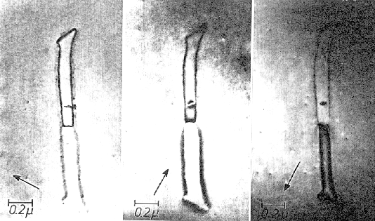
Next we will see how a dislocation
loop can be analyzed. |
|
|
Shown are dislocation loops of the "A-swirl defects" imaged
with two different diffraction vectors (drawn in as arrows) and a
+g/–g pair. In the first image, the contrast of the lower
dislocation loop has disappeared (the fuzzy line is due to the precipitates
along the dislocation line). The two pictures on the right show the lower loop,
the image is wide or narrow, depending on the sign of the diffraction vector
g. |
|
|
|
|
|
|
|
|
|
|
|
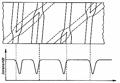
This is an important effect because it allows to
analyze the nature of a dislocation loop as schematically illustrated below.
The image of the loop lies inside or outside the geometric projection; upon
reversing the sign of g or b (and this means switching from
vacancy to interstitial type), the image switches between the two
extremes. |
|
|
|
|
|
|
|
|
|
|
|
For a given geometry it is possible to predict if
the contrast is "inside" or "outside"; the nature of a loop
may thus be determined. But beware! There are many possibilities of committing
a sign error! Printing the negative with emulsion side up or down, e.g., will
exchange the signs and turn a vacancy loop into an interstitial loop or vice
versa. |
|
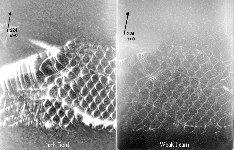
The next example compares regular
dark field and weak-beam conditions. The object is a very dense dislocation
network with a complicated structure which we will encounter again in the
context of grain boundaries. |
|
|
|
|
|
|
|
|
The weak-beam image on the left shows a lot more
detail, but the signal to noise ratio is rather bad. This is about the limit of
the resolution obtainable under weak beam conditions. |
|
|
In the link, a
comparison between weak-beam
conditions and bright field can be found. |
|
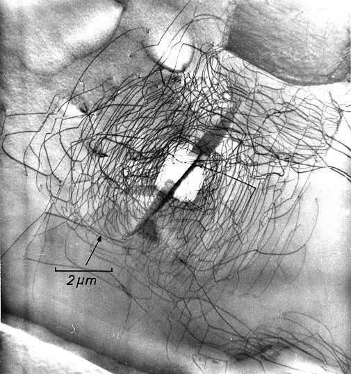
The last picture shows conventional
bright field imaging. |
|
|
The tip of a probe produced some mechanical damage
in the emitter area of a transistor in an integrated circuit (the bright square
area in the center of the tangle). A microcrack was generated (the elongated
black shape); upon heating in the next processing cycle the dislocation tangle
was formed to relieve the stress. |
|
|
|
|
|
|
|
|
|
|
|
By tilting the specimen while keeping the imaging
conditions constant (this involves a rotation around the diffraction vector), a
second picture can be obtained under a somewhat different imaging direction.
The two pictures can be viewed in a stereo viewer and will produce the full
three-dimensional glory of the structure. |
|
More examples can be found in the
links |
|
|
Weak-beam image of a dislocation network
involving partial dislocations under different diffraction conditions
Unknown ribbon defect in
Si, showing difficulties in interpretation
Radiation damage in
Co showing possibilities of interpretation
FeSi precipitates in
Si
Prismatic punching of
dislocation loops from precipitates
Helix dislocations produced
by climb of screw dislocations
Dislocations in TiAl
being pinned by debris
PtSi on Si
showing the power of diffractions
patterns (for
another
example use the link)
Comparison weak beam - bright
field |
© H. Föll
© H. Föll