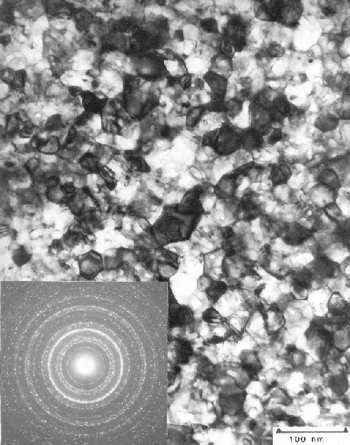
| Metal Silicides play an important role in microelectronics. PtSi has been used in bipolar technology for quite some time; other silicides abound in MOS techniques. | |||
| Silicides are usually formed by evaporating a thin metal layer (here Pt) on a Si substrate, which is subsequently annealed at some high temperarture; say 800 oC. Silicides form by solid state reactions, the picture below shows one result. A fine grained film of PtSi has formed in this case. | |||
| The picture illustrates that in polycrystalline materials the images are dominated by grain boundaries. The contrast conditions are pretty random and different in every grain. Not much can be seen. | |||
| The diffraction picture, shown as an insert, often provides more important information than the direct image. It consists of many reflexes arranged in rings; typical for polycrystalline materials. Every spot comes from one grain that happens to meet the Bragg condition for the particular reflex. | |||
|
|||
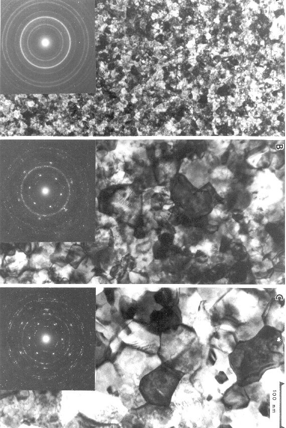
| Increasing the annealing time or the annealing temperature makes the PtSi film more coarse grained; this is easily seen in the sequence below. But only the diffraction image shows that an epitaxial relationship to the Si substrate develops at high temperatures. | |||
|
|||
| In the top picture the grains are so small that their diffraction pattern forms structureless rings. In the two lower pictures, however, some grains are still at a random orientation producing reflexes somewhere on the rings, but many grains have the same orientation producing strong spots at the same position -there is an epitaxial relationship to the substrate. This can be seen by closely inspecting the diffraction pattern: The spots from the epitaxial PtSi grains are almost coincident with the Si spots. | |||
![]() 6.3.2 Examples and Case Studies for Dislocations
6.3.2 Examples and Case Studies for Dislocations
![]() 6.3.3 Stacking Faults and Other Defects
6.3.3 Stacking Faults and Other Defects
© H. Föll