|
Two-dimensional defects like stacking
faults, but, to some extent also grain- and phase boundaries, give rise to some
special contrast features. |
|
 |
Stacking faults are best seen and identified under dynamical
two-beam condition; i.e. the Bragg condition is exactly met for one point in
the reciprocal lattice. |
|
|
This automatically implies that the diffracted beam, if seen
as the primary beam, also meets the Bragg condition; it is diffracted back into
the primary beam wave field. |
|
|
This leads to an oscillation of the intensity between the
primary and the diffracted beam as a function of depth in the sample; the
"wave length" of this periodic intensity variations is called the
extinction length
ξ. |
|
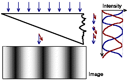
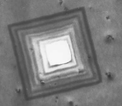
For a wedge-shaped specimen, the
intensity of the primary or diffracted wave thus changes with the local
thickness; it goes through maxima and minima. |
|
|
The illustration shows the resulting image: a system of black
and white fringes, called thickness fringes or thickness contours is seen on the
screen.On top a schematicdrawing, on the bottom the real thing. In this case it
is an etch pit in a Ge sample which is the usual inverted pyramid with
{111} planes. |
|
|
|
|
|
|
|
|
|
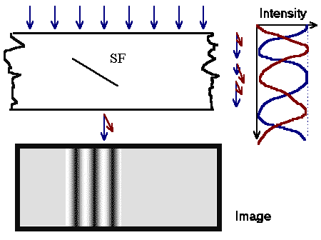
A stacking fault can be seen as the
boundary between two wedge shaped crystals which are in direct contact, but
with a displacement R along the wedge. |
|
|
As a result, the two fringe systems resulting from the two
wedges do not fit together anymore. A new fringe system develops delineating
the stacking fault; we see the typical stacking fault fringes |
|
|
|
|
|
|
|
|
|
|
|
Again, getting all the signs right, the nature of the stacking
fault can be determined. If intrinsic stacking faults under some imaging
conditions would start with a white fringe, extrinsic stacking faults would
start with a black one. Reversing the sign of the diffraction vector
g or the displacement vector R changes white to
black and vice versa. |
|
If more kinematical conditions are
chosen, the amplitude of the intensity oscillation decreases; the stacking
fault contrast assumes an average intensity that is usually different from the
normal background intensity - stacking faults appear in grey. |
|
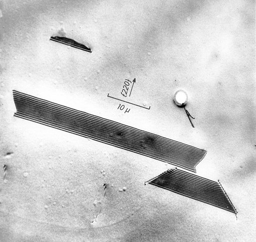
A few examples: The picture below shows three
defects that behave as predicted and could be stacking faults. Indeed, the
small defect in the top half and the very large defect are stacking faults. The
smaller defect in the bottom part, however is a micro
twin. This is not evident from one picture, but can be concluded from
contrast
analysis. |
|
|
|
|
|
|
|
|
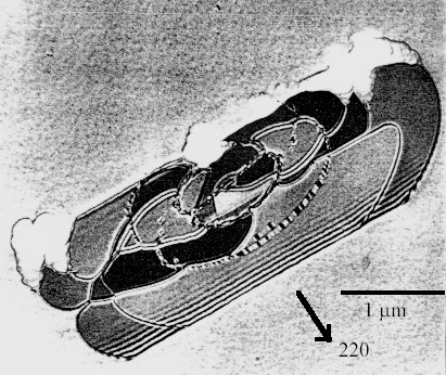
The next picture shows a complicated arrangement
of several stacking faults: |
|
|
|
|
|
|
A whole system of overlapping
oxidation induced stacking
faults in Si. The biggest loop was truncated by the specimen
preparation; the fringe system where the stacking fault intersects with one
surface is clearly visible. |
|
The other surface was preferentially etched; the etch pits
down the (Frank) dislocation lines are clearly visible. |
|
The overlap of several stacking faults leads to changing
background contrasts - from black to no contrast (whenever multiples of three
stacking faults overlap) to almost white. |
|
|
|
|
|
Similar if less complicated contrast effects were
already encountered in illustrations given before in the
context of point defect agglomeration. |
|
|
More examples of a typical
oxidation induced stacking faults in
Si (OSF) are
given in the link |
|
But there are limits to TEM analysis:
Sometimes defects are observed which resist analysis.
One example is shown in the
link; another one we will encounter in the next subchapter. |
|
|
|
The strain-induced contrast of
dislocations due to local intensity variations in the primary and diffracted
beams and the fringe contrast of stacking faults due to local phase shifts of
the electron waves, if taken together, are sufficient to explain
(quantitatively) the contrast of any defect. |
|
|
It may get involved, and not everything seen in TEM
micrographs will be easily explained, but in general, contrast analysis is
possible and the detailed structure of the defect seen can be revealed within
the limits of the resolution (you cannot, e.g., find a
kink in a
dislocation (size ca. 0,3 nm) with a typical kinematical bright field
resolution of 5 nm). |
|
In the links a gallery of micrographs
is provided with a wide spectrum of defects. Bear in mind that most examples
are from single crystalline and relatively defect free Silicon. The images of
regular poly-crystalline materials would be totally dominated by their grain
boundaries (see the examples at the end of the list). |
|
|
Small
dislocation loops in Cobalt produced by ion-implantation. |
|
|
Precipitates in
Silicon with dislocation structures. |
|
|
Needle
shaped FeSi2 precipitates in Si; the bane of early
IC technology. |
|
|
Helical
dislocations resulting from the climb of screw dislocations. |
|
|
Bowed-out
dislocations in a TiAl alloy; kept in place by point defects and
small precipitates. |
|
|
A thin film of
PtSi on Si as an example of the "real" world of
fine-grained materials. |
|
|
Overview of
TiAl as an example of a specimen with a high defect density. |
|
|
|
© H. Föll