|
High-Resolution TEM (HRTEM) is the ultimate tool in imaging
defects. In favorable cases it shows directly a two-dimensional projection of
the crystal with defects and all. |
|
 |
Of course, this only makes sense if
the two-dimensional projection is down some low-index direction, so atoms are
exactly on top of each other. |
|
The basic principle of HRTEM
is easy to grasp: |
|
|
Consider a very thin slice of crystal that has
been tilted so that a low-index direction is exactly perpendicular to the
electron beam. All lattice planes about parallel to the electron beam will be
close enough to the Bragg position and will diffract the primary beam. |
|
|
The diffraction pattern is the Fourier
transform of the periodic potential for
the electrons in two dimensions. In the objective lens all diffracted beams and
the primary beam are brought together again; their interference provides a
back-transformation and leads to an enlarged picture of the periodic
potential. |
|
|
This picture is magnified by the following
electron-optical system and finally seen on the screen at magnifications of
typically 106. |
|
The practice of HRTEM,
however, is more difficult them the simple theory. A first illustration serves
to make a few points: |
|
|
|
|
|
|
|
|
|
|
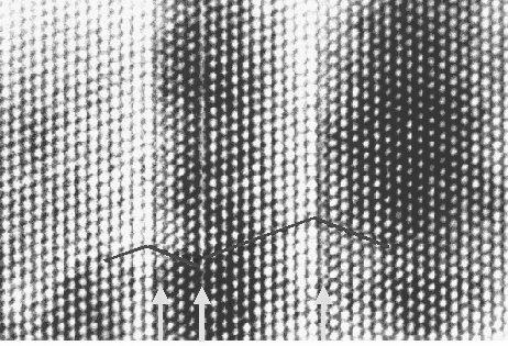
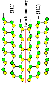
The image shows one of the first HRTEM
images taken around 1979; it is the <110> projection of the
Si-lattice; a schematic drawing is provided for comparison. It also
contains a few special grain boundaries, called twin boundaries. |
|
We notice a few obvious
features: |
|
|
Instead of two atoms we only see a dark
"blob." |
|
|
Or does the dark blob signal the open channels in
the lattice projection? There is actually no way of telling from just one
picture. |
|
|
The twin boundaries look fine in comparison to the
drawing at a first glance. Looking more closely, one realizes that there are a
few unclear points: The yellow arrow points to "fuzzy" lattice planes
to the right (or left) of the boundary. Following a fringe across the boundary
seems to result in an offset - what does it mean? But what should we expect
defects (in this case the twin boundaries) to look like? After all, they
destroy the periodicity of the lattice and it is not obvious what Fourier
transforms of defects will produce in general cases. |
|
The last point is easy to solve: Just
do a simulation of a defect (i.e. calculate the image for an assumed slice of a
crystal with all atoms at the proper positions), but mind the points mentioned
below! These are the limitations to HRTEM stemming from the non-ideality
of the instrument and the specimen: |
|
|
The specimen is not arbitrarily thin! If the
thickness is in the order of the extinction length, some reflexes may have very
small intensities because they were diffracted back into the primary beam. The
objective lens then will not be able to reconstruct the spatial frequencies
contained in these reflections; the image looks like a different lattice. |
|
|
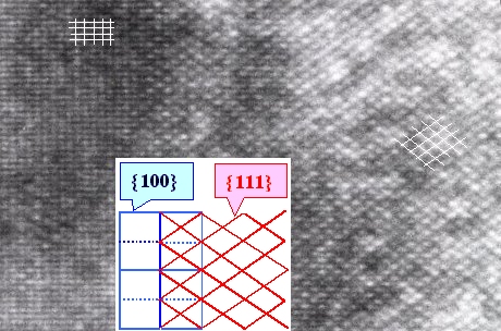
This can be nicely seen in a HRTEM image of
Si where the thickness of the sample increases continuously: |
|
|
|
|
|
|
|
|
|
|
|
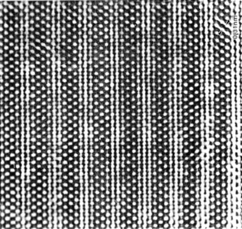
The inset shows the lattice in <110>
projection; an elementary cell is given by the large rectangles formed by solid
blue lines. |
|
|
On the right hand side of the picture, all
reflections are excited; the very strong {111} reflections dominate the
image and the {111} lattice planes (indicated by white lines) are most
prominent. On the left hand side the thickness happens to be in a region where
the {111} reflections are weak; the {400} type reflections
dominate ({100} etc. are "forbidden" in the diamond lattice).
The lattice appears rectangular. |
|
In principle, this can be calculated,
too, without much problems. What is much more problematic is the "contrast transfer function"
of the objective lens. |
|
|
If we consider the objective lens to be some kind
of amplifier that is supposed to amplifies (spatial) frequencies in the input
with constant amplification and without phase distortion, the objective lens is
a very bad amplifier. It has a frequency
response that is highly nonlinear, the amplification drops off sharply for high
(spatial) frequencies (meaning short distances). In other word, the resolution
is limited (to roughly 0,1 nm in good TEMs); you cannot see
smaller details. |
|
|
But worse yet, around the resolution limit, the
objective lens induces strong phase shifts as a function of several parameters
(the most important one being the focus setting); this influences the
interference pattern which will define the image. |
|
Both effects together can be
expressed numerically in the contrast transfer function of the lens. If you
know that function (for every picture you take) you may than calculate what the
image would look like for a "perfect" lens with a certain resolution
limit; or somewhat easier, you calculate what a crystal with the defects you
assume to be present would look like in your particular microscope with the
contrast transfer function that it has. |
|
Neither approach is very easy; the
amount of computing needed can be rather large. Worse, you must determine parts
of the contrast transfer function experimentally; and that involves taking
several images at different focus settings. Still, HRTEM images provide
the ultimate tool for defect studies. They are perfectly safe to use without
calculations if you obey two simple rules: |
|
|
Only look at pictures where the perfect part of
the crystal looks as it should. After all, you usually know what kind of
material you are investigating. So if the image of a diamond structure looks
like the left part of the illustration above; throw it away (or at least use
with care). It it looks like a diamond strucure you can't go totally wrong in
interpreting the picture. |
|
|
Only draw qualitative conclusions (e.g. there is a
dislocation in this GaAs specimen!); never draw quantitative conclusion
(e.g. it ends at a Ga atom!) without calculating the image. |
|
Some more details to HRTEM
imaging can be found in the (German)
article in the
link |
|
Three examples may serve to
illustrate HRTEM here; more will be found in the upcoming chapters. |
|
|
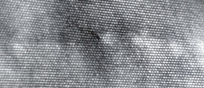
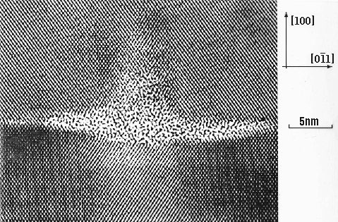
The first picture shows a small angle
grain boundary in Si. This was the first picture of this kind; it only
can be interpreted qualitatively; the contrast transfer function was not known.
What we see beyond doubt are several lined-up dislocations which constitute a
boundary - the top half of the lattice is tilted with respect to the bottom
half. |
|
|
|
|
|
|
|
|
|
|
|
The next picture (from W. Bergholz) shows an
SiO2 precipitate in Si. Again, a qualitative
interpretation is neither possible nor necessary. It is clear that the
precipitate, albeit very small, is not spherical |
|
|
|
|
|
 |
| Courtesy of W. Bergholz |
|
|
|
|
|
|
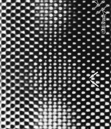
The last example shows
quantitative HRTEM (from W. Jäger) Careful imaging under various
conditions, extraction of the contrast transfer function and prodigious
computing allowed not only to image a sequence of Si - Ge multilayers
produced by molecular beam epitaxy (MBE), but to identify the positions
of the Si and Ge atoms. The first picture shows an overview. The
brighter regions indicate the Ge layers, but it is not clear exactly how
the lattice changes from Si to Ge. |
|
|
|
|
|
 |
| Courtesy of W. Jäger |
|
|
|
|
|
|
This image also demonstrates the progress made in
building electron microscopes. The "old" pictures shown above were
taken with a the best general-purpose TEM available around 1980
(Siemens Elmiskop 102). The last pictures were taken with a TEM
optimized for high resolution around 1995. |
|
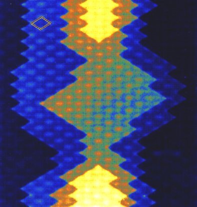
Next a comparison between an enlarged part of the
Ge/Si stack is shown together with a quantitative evaluation of this and
other pictures obtained at different focus settings from W. Jaeger and his
group. The color codes defined Ge concentrations and a very clear
representation of the multilayer sequence is obtained. |
|
|
|
|
|
 |
 |
| Courtesy of W. Jäger |
|
© H. Föll