|
The basic idea behind preferential etching is to mark defects
intersecting the surface by a small pit or groove, so they become visible in a
microscope. |
|
 |
Start with a well polished surface that does not
show any structures in a light
microscope (including high magnifications and sensitive modes, e.g.
phase or interference
contrast |
|
|
Find an etching solution that dissolves your
material much more quickly around defects than in perfect regions (that is the
tricky part). |
|
|
Expose (= etch) your sample in this solution for
an appropriate amount of time. What happens will be something like this: |
|
|
|
|
|
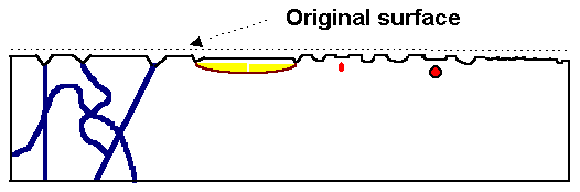 |
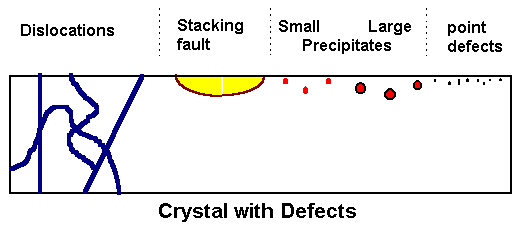
Model crystal with several kinds of defects intersecting the
(polished) surface on top,
and surface structure after preferential etching of defects. |
|
| |
|
|
|
After preferential etching you obtain
well developed etch pits (actually something
looking more like pointed etch cones) at the intersection points of
dislocations (including partial dislocations) and the surface and
etch grooves at the intersection line of
grain boundaries and stacking faults with the surface. Precipitates will be
shown as shallow pits with varying size, depending on the size of the
precipitate and its location in the removed surface layer. Areas with high
densities of very small precipitates may just appear rough. Two-dimensional
defects as grain boundaries and stacking faults may be delineated as grooves.
|
|
|
There is a certain problem with
grain boundaries, however: They may also be delineated, i.e. rendered visible, with chemicals
that do not preferentially etch defects, but simply dissolve the material with
a dissolution velocity that depends on the grain orientation (this is the rule
and not the exception for most chemicals). |
|
|
In this case grain boundaries show up as steps and not as grooves. Small steps and grooves, however, look very
similar in a light microscope and may easily be mixed up. |
|
You may think: So what! - in any case
I see the grain boundary. Well, almost right, but not quite - there are
problems: |
|
|
Grain boundaries separating two grains with
similar orientation with respect to the surface would not be revealed. |
|
|
The delineation of grain boundaries obtained
under uncertain etching conditions suggests that you delineated
all defects - but in fact you did not.
Delineation of grain boundaries thus must not be taken as an indication that
the etching procedure works and there are no defects, because you don't see
any! |
|
Before we look at examples and case
studies, two important points must be made: |
|
1. Defect etching for many
scientists is a paradigm for "black
art" in science. There are good reasons for this view: |
|
|
Nobody knows how to mix a preferential etching
solution for some material from theoretical concepts. Of course you must look
for chemicals or mixtures of chemicals that react with your material, but not
too strongly. But after this bit of scientific advice you are on your own in
trying to find a suitable preferential etch for your material. |
|
|
Well-established preferential etching solutions
usually have unknown and poorly understood properties. They sometimes work only
on specific crystallographic orientations; their detection limits for small
precipitates are usually unknown; they may also depend on other parameters like
the doping level in semiconductors; and so on. |
|
2. Defect etching in practice is more art
then science. |
|
|
Beginners, even under close supervision by a
master of the art, will invariably produce etched samples with rich structures
that have nothing to do with defects - they produced so-called
etch artifacts. It takes some
practice to produce reliable results. |
|
|
But: Defect etching still
is by far the most important and often most sensitive technique for observing
and detecting defects! |
|
There are many routine procedures for
delineating the defects structure of metals by etching. Here we will focus on
defects etching in Silicon; which is still the major technique for defect
investigations in Si technology. Some
details and peculiarities of
defect etching in Si can be found in the link. In what follows we
look at the power and possible mechanisms of preferential etching in the
context of examples from recent research. |
|
|
|
The name "Swirl defects"
was used for grown-in defects in large Si crystals obtained by the
float-zone technique in the seventies. |
|
|
Swirl defects are a subspecies of
what now is known as "bulk micro
defects" (BMD); they are
nothing but agglomerates of the point defects present in thermal equilibrium
near the melting point with possible influences of supersaturated impurities
still present in ultra clean Si (only oxygen and on occasion carbon).
|
|
|
Whereas the relatively large swirl
defects are no longer present in state-of-the-art Si crystals, point
defect agglomerates and oxygen precipitates still are - there is no way to
eliminate the equilibrium defects! BMDs are a major concern in the
Si industry because they cause malfunctions of integrated circuits. The
link leads to some recent papers on point defects and
BMDs in Si crystals. |
|
|
|
|
Most of the examples relating to
Si are taken from the work of B.O. Kolbesen (formerly at Siemens; now
(2001) at the University of Frankfurt). |
|
|
|
|
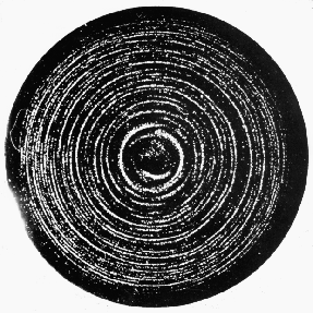
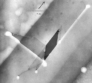
The name "swirl" comes from the spiral
"swirl-like" pattern observed in many cases by preferential etching as shown on the right. |
|
|
Close inspection revealed two types of etch
features which must have been caused by different kinds of defects. Lacking any
information about the precise nature of the defects (which etching can not
give), they were termed "A-" and "B-swirl
defects". More pictures and information in the
link |
|
|
|
|
Understanding the precise nature of
swirl defects was deemed to be very important for developing crystal growth
techniques that could avoid these detrimental defects. |
|
|
But etching alone can not give
structural data, and other techniques as, e.g., transmission electron
microscopy, could not be applied directly because the densities of swirl
defects was too small (the likelihood of having a defect in a typical
TEM sample was practically zero). A combination of a special etching
technique and TEM, however, could give the desired results. |
|
|
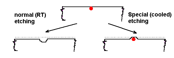
The power and the "black
art" component of defect etching is nicely demonstrated by the following
development: A "special etch" which was simply the old solution, but
cooled to about freezing temperatures, did not produce etch pits (and thus
remove the defect) for A-swirls, but hillocks (still containing the defect).
|
|
|
|
|
|
|
|
|
|
|
The hillocks identified the precise
location of the A-swirl defect. A special preparation technique rendered
the areas containing hillocks transparent for TEM investigations, and
the structure of A-swirls defects could be identified. They consisted of
dislocation loop arrangements that were generated by the agglomeration of
interstitials. This gave the first direct evidence that self-interstitials are
important in Si. |
|
|
B-swirl defects could not be
identified with this technique - their nature is still not clear. |
|
|
More about swirl defects and the
application of preferential etching can be found in an original paper (in
German) in the link. |
|
|
|
|
The manufacture of
integrated
circuits (IC) involves many
processes prone to introduce defects in the more or less perfect starting
crystal. |
|
|
All high temperature processes induce temperature
gradients which lead to stress and thus to a driving force for plastic
deformation. Since the starting material is dislocation free, the decisive
process is the generation of the first dislocations which is much easier if
small precipitates or dislocation lops are already present. |
|
|
Thermal oxidation introduces Si
interstitials with a strong tendency to agglomerate into stacking fault loops,
so-called
oxidation induced stacking faults (OSF). |
|
|
All processes tend to induce trace amount of
metals which will diffuse into the Si and eventually precipitate. |
|
|
Ion implantation destroys the lattice to a large
degree up to complete amorphization. Even upon careful annealing some defects
may be left over. |
|
As a general rule, all defects in the
electronically active part of an IC (roughly the the first 5 µm
- 10 µm of the wafer) are deadly for the device. They have to be
avoided and that means that they have to be monitored first. The method of
choice is preferential etching. |
|
Lets look at an example |
|
|
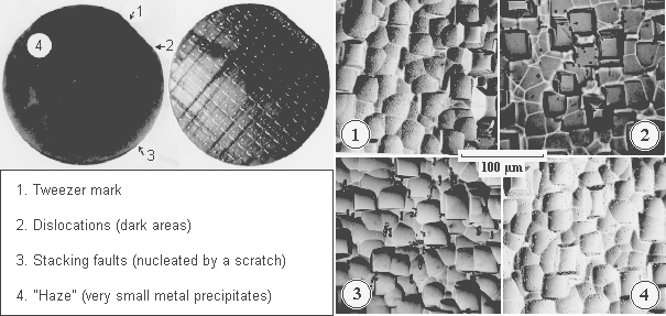
The pictures show a Si wafer with several
defect types introduced during very early stages of processing.
Details are provided in the
link. |
|
|
|
|
|
|
|
|
|
|
A few more example are provided in
the links. They might be a bit unconvincing, but be aware that looking into an
actual microscope gives you much more information than what can be captured in
a few pictures. |
|
|
Development of stacking faults in bipolar
transistors |
|
|
Precipitates and other defects |
|
We are now able to
compare weaknesses and strength of preferential etching for defect detection:
|
|
|
|
|
| Strength |
Weaknesses |
- Simple and cheap
- Rather sensitive
- Applicable to large areas
- Needs no special knowledge (as e.g. TEM
|
- Black art
- Detection limit unclear
- What you see must be interpreted
- Problems with artifacts
- Mechanism not clear
- No systematic developments of etches
|
|
|
|
|
|
One last example
serves to illustrate the "what you see must be
interpreted" point. Shown is a complex defect composed of
stacking faults, dislocations and possibly a
microtwin in full splendor
in a TEM micrograph (left), and a schematic outline of what the
preferential etching would look like in an optical microscope. |
|
|
|
|
 |
 |
| TEM micrograph |
What you would see with preferential etching
Since the etch pits are smaller than 1 µm,
they only would appear as blurred black-white structures |
|
|
|
|
|
|
|
The planar defects are inclined in a thin foil;
what one sees is the projection. One surface was preferentially etched; at the
intersection of the defect with this surface the etch features can be seen as
bright areas (the sample thickness is smaller at etched parts). The stacking
fault lines will be clearly visible in an etch picture, but the various
dislocations involved are etched with different strengths. |
|
|
It will not be possible to conclude from the etch
pattern alone on the complexity of the actual defect. This stacking fault
assembly corresponds to some extent to the etch pattern shown in the
development of stacking faults in bipolar patterns given
in the link. |
|
Chemical etching on occasion is
driven to extremes - simply because there is no alternative. The link leads to
an advanced module, where a particular
tricky case study is
presented |
|
|
|
Chemical etching, as any chemical
dissolution process, is an oxidation-reduction process expressed in chemical
terms. Carriers are transferred from the substrate to the chemicals, new
compounds form and go into solution. The paradigmatical model for these
processes is anodic dissolution under
applied bias, where the carriers are supplied by a controlled external power
source. Maybe a way towards the understanding of preferential etching comes
from the electrochemistry of the specimen? |
|
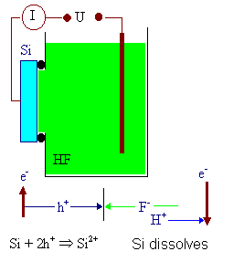
Anodic etching has been studied to
some extent in Silicon. It leads to a rather unexpected wealth of effects that
are at the focus of some
current resarch projects. The
experiment is simple: |
|
|
Bias the (p-type) Si sample positively in some
electrolyte that contains hydrofluoric acid (HF). The HF itself
is "contacted" by some inert electrode, e.g. a Pt wire, which
establishes a closed circuit. |
|
|
The Si-HF- junction behaves to some extent like a
Schottky junction;
current flow, however, is always accompanied by a chemical reaction. The
current density first increases steeply with the applied bias, then reaches a
maximum (called jPSL; PSL stands for
"porous Si layer") and decreases again (that is when the
analogy with a Schottky junction fails), goes through a second maximum (called
jox) and finally starts to oscillate . |
|
|
In the "forward" regime of the junction, the
reaction is the dissolution of Si (in reverse condition it is
H2 evolution). |
|
If a polished specimen that was
subjected to a current density considerably smaller than the first peak value
is inspected after some etching time, its defect will be revealed in a way
reminiscent of purely chemical etching. This can be understood (in parts) by
considering current flow in terms of
diffusion current and generation
currents as introduced in basic pn- (or Schottky)-junction theory.
The major ingredients for anodic etching are shown below. |
|
|
|
|
 |
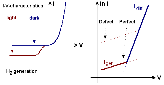 |
Basic experimental set-up, current flow
and chemical reaction |
Measured I-V-characteristic and theoretical plot of
ln I vs.V with diffusion
and generation currents. Around a defect the generation current is larger than
in perfect Si. |
|
|
|
|
|
|
|
Preferential defect etching thus can
be understood in terms of current flow: At small current densities the
generation currents are larger than the diffusion current, the area around
electronically active
defects (i.e. defects that generate carriers) should be etched more deeply and
etch pits should appear. At larger current densities the differential etch rate
should disappear. The experiments support this view to some extent; the link
contains some results |
|
|
General results of anodic etching |
|
The consideration of the influence of
defects on a Schottky junction suggests a different approach to the detection
of electronically active defects: Measure the local leakage current or
radiation induced current of a junction. This can be done by injecting current
locally by an electron beam through a thin Schottky barrier while measuring the
induced current. Electronically active defects will recombine more carriers
than the defect-free regions, the current will be locally reduced. |
|
|
This method exists and is called "electron beam induced
current" technique (EBIC) if a scanning electron
microscope is used as the basic instrument. If a scanned light beam is used, we
have the "light beam induced
current" technique or LBIC; the mainstay of solar cell
development with poly crystalline Si. |
|
|
The
principle of EBIC is
shown in the link. |
|
|
If one compares anodic etching, chemical etching
and EBIC, much can be learned about defects and the detection methods,
but many questions remain open. Some examples are given in the link |
|
Anodic etching is still a virulent
research issue within the context of the
general
electrochemistry of semiconductors. |
© H. Föll