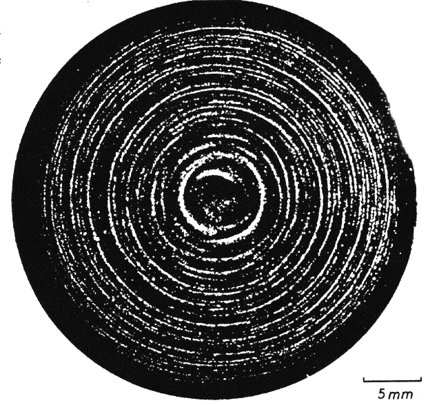
| Swirl defects were discovered in the seventies in large dislocation-free Si crystals grown for micro electronic applications. They occur in two variants, the so-called A-swirl and B-swirl defects. The following picture shows a photography of a Si wafer that was preferentially etched to delineate the defects obtained by illuminating from the side (so that only light scattered at the defects enters the lens of the camera). | |||
| The typical spiral or swirl-like pattern explains the name of the defects. | |||
|
|||
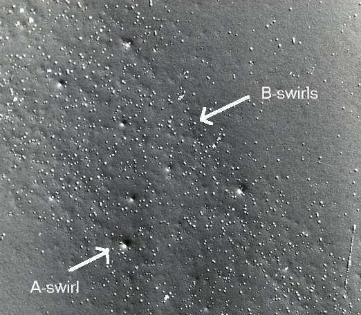
| Looking at the etch pattern with a microscope at high magnifications shows that there are a lot of small defects (the B-swirls; white dots) and a much smaller number of larger defects (A-swirls; the black-white contrasts). Quantitative evaluation of the micrograph shows that the B-swirls are delineated as small and shallow pits whereas the A-swirls are delineated as hillocks. | |||
|
|||
| Swirl defects are generated by the agglomeration of point defects while the crystals cools. The Si crystal growing industry soon learned how to grow crystals without swirl defects - without ever understanding precisely what they were. | |||
| But that did not mean that the crystals were defect free - it only meant that the methods employed then did not detect what was there. With new methods, defects reappeared, now called D-defects and bother the chip industry. | |||
| More about swirls can be found in a original research paper (in German) in the link. | |||
![]() 1.3.3 The larger View and Complications
1.3.3 The larger View and Complications
![]() 6.1.1 Observation of Dislocations and Other Defects
6.1.1 Observation of Dislocations and Other Defects
![]() Etch Pattern of Swirl Defects in Silicon
Etch Pattern of Swirl Defects in Silicon
© H. Föll