|
The results obtained with anodic etching depend on the current density
used. For small current densities there is a tendency to reveal only
electronically active defects, whereas at higher current densities all defects
are etched. This can be seen in comparison with "normal" chemical
etching and with EBIC |
|
|
|
|
|
|
|
|
|
|
|
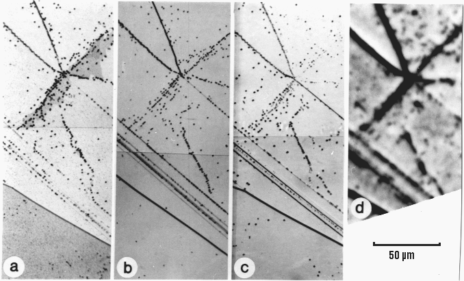
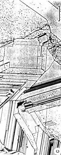
The pictures show the same area of a solar
Si sample (always repolished after one experiment): |
|
 |
a) Anodically etched at small current
density. Only some of the twin boundaries at the lower half of the picture are
faintly delineated. |
|
|
b) Anodically etched at high current
density. The twin boundaries at the lower half of the picture are
delineated. |
|
|
b) Chemically etched. The twin boundaries
are partially delineated. |
|
|
c) EBIC Micrograph. Upon close
inspection, it is mostly compatible with a). |
|
This gives the impression that anodic etching at
small current densities reveals only electronically active defects whereas at
higher current densities it shows all defects. This can be clearly demonstrated
in another optimized comparison below |
|
|
|
|
|
|
|
|
|
|
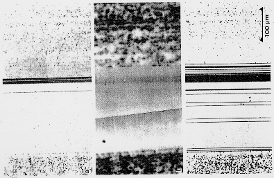
Left, the etching structure obtained at small, on
the right with high current densities. The EBIC picture is shown in the
middle. It is obvious that only a few twin boundaries show up at low current
densities and in the EBIC mode. |
|
One more example confirms this result |
|
|
|
|
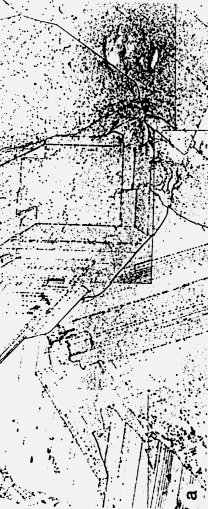 |
| Low current density |
|
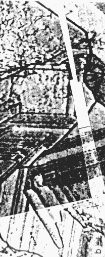 |
| EBIC |
|
 |
| High current densitiy |
|
|
|
|
|
|
© H. Föll