|
With the development of the 4
Megabit Dynamic Random Access Memory (DRAM) and of the eighties, a
new process was introduced into Si technology:
Trench
etching for trench capacitors. |
|
 |
A trench,
contrary to the literal meaning of the word, is simply a small hole - typically 1 µm in diameter and
(6 - 8) µm deep. It is made to provide a large area for the
capacitor while still using only about 1 µm2 in
"real estate" on the chip surface. |
|
|
All kinds of problems were encountered with the
performance of the trench capacitors, some - maybe - caused by dislocations
ending inside the trench. |
|
|
Since there are about 4 ·
106 trenches on one chip, and some 100 chips on a wafer,
looking with an electron microscope at a few trenches will not do much good -
you will turn to defect etching, |
|
There is a clear question to the analytical people
then: Are there dislocations inside the trench, and if yes, does his correlate
with electrical performance? Well, Wendt, Sauter and
Kolbesen of Siemens AG answered this question in an elegant, if
tricky way with chemical etching. Here is what they did. |
|
|
If you etch your wafer with some defect etch, you
may obtain pictures like the following one |
|
|
|
|
|
|
|
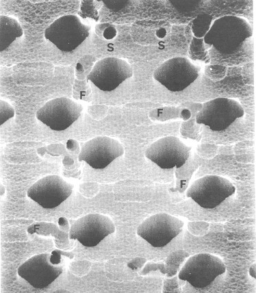
This is a SEM picture, because you would not see very
much with a light microscope - the big holes being the trenches are just about
1 µm across. In fact, while you would detect the relatively shallow
dislocation etch pits marked by "F", you would miss the sharp
little holes marked with "S". |
|
Well, you see that there are dislocations ending at the
surface. What you do not see is if there are dislocations ending on the surface
of a trench; i.e. inside the hole. If you
look real close, you might on occasion find something as shown below: |
|
|
|
|
|
|
|
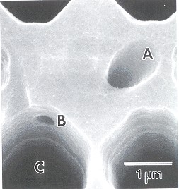
OK, here you have the etch pits of a dislocation that starts
at the surface at "A" and ends obviously inside the trench at
"B" - but still rather close to the surface. |
|
How about deeper down in the trench? How do you look inside a
1 µm trench (with any method)? |
|
|
|
|
Here is the solution: |
|
|
- Etch the whole wafer, producing etch pits inside the trench if there is a
dislocation.
- Coat everything with a thin layer of Si3N4.
- Etch off all of the Si, leaving only the
Si3N4 layer intact.
- Inspect the Si3N4 layer. It is a kind of
"negative" of the trench structure which now is easily inspected.
|
|
|
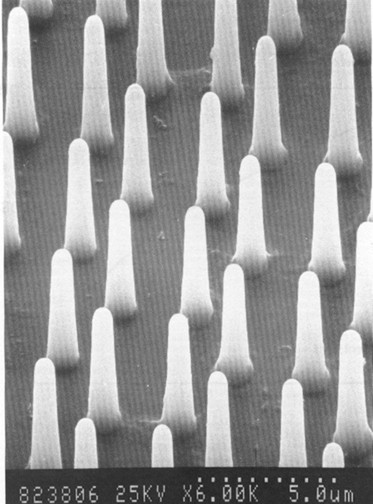
Pretty tricky (and by far not as easy as it
sounds). Here are some results (the "stripes" are artifacts from
image processing) |
|
|
|
|
|
|
|
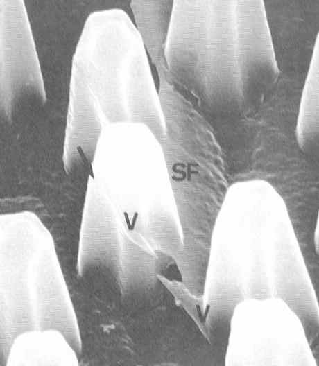
The inverted trench structure - pretty perfect in this
case. |
|
|
|
|
|
|
|
|
|
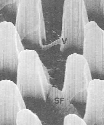
The structure marked "V" clearly results from
a dislocation running from a trench to its neighbor. |
|
The structure marked "SF" actually shows a
stacking fault. |
|
|
|
|
|
|
|
|
|
Same thing here - a prominent stacking fault (and a
dislocation). |
|
So we have stacking faults, not just dislocations at work
here! This is a major finding, that would have been practically unavailable
with other methods. |
|
It is a major finding, because now we have a pretty good idea
where the defects are coming from: We most likely deal with a new kind of
oxidation induced stacking fault, and
that give us a clear idea of what needs to be done to get rid of those
defects. |
|
|
|
© H. Föll