|
Playing with models of a perfectly
fitting phase boundary between a hexagonal and a cubic lattice, one realizes
quickly that steps can be incorporated without problems and without dislocations as long as the step height
comes in multiples of 3 (in units of the translation vectors of the
CSL). This, together with some other cases, is shown below: |
|
|
|
|
|
|
|
|
|
|
 |
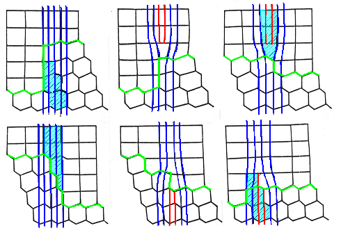
The left two pictures show pure
steps (or coherent steps). For
ease of interpretation, some lattice planes
of the DSC
lattice are shown in blue; ending lattice planes of the DSC lattice
are red. Ending lattice fringes, as seen
on a HRTEM micrograph, are indicated in light blue - note that they are
not the same thing as lattice planes. The phase boundary itself is shown in
light green. |
|
|
Included in the drawing are also two pure DSC lattice dislocations (middle
pictures). They are true dislocations because they can be constructed with the
Volterra method as
demonstrated before, and they have the
1/r
stress field that is a hallmark of dislocations. Sometimes they are called
coherency dislocations. |
|
|
Finally, a mix of pure dislocations and pure steps is shown on
the right. It is evident that steps going just one plane up or down must be a
mix of pure steps and pure dislocations. The same is true for steps going
4 planes up or down and so on. These dislocations are sometimes called
anti-coherency
dislocations. |
|
|
Note that there is no way of having a combination of pure
steps and dislocations with step height zero. |
|
An unexpected
property emerges: Pure steps (sometimes also
called coherent ledges) show ending
lattice fringes in a HRTEM micrograph, whereas true dislocations in this
case are not associated with ending lattice
fringes. |
|
|
Where does that leave us? Is Franks formula,
which after all counted Burger vectors in a circuit not unlike the one
shown before, not applicable to
non-planar boundaries? Why can we see ending lattice fringes in a TEM
picture and there is no dislocation? |
|
|
Well, ending lattice fringes (again note we call it lattice fringe on purpose) are not lattice planes, and at a grain- or phase boundary all lattice planes of one kind end and some of a new
kind start. The fact that some visible fringes appear to be continuous in a
"fuzzy" projection of the lattices, has no particular meaning in
itself. Of course, one lattice plane ending in one crystal may give rise to a
lattice fringe ending on a micrograph, too, and thus signify an edge
dislocation, but this must not be
generalized. |
|
We may, however, make an important
generalization of a different kind: A semi-coherent phase or grain boundary, in
general, needs at least two qualitatively different
kinds of defects in its interface: |
|
|
Pure DSC-lattice
dislocations (generally associated with an intrinsic step), and |
|
|
Pure steps
(without dislocation character, i.e. without a long range stress field). |
|
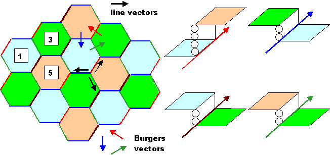
In general both defects are required as we will see if we
now compose a (hexagonal) dislocation network in a Σ = 3 boundary. |
|
|
Whereas the dislocation network has a perfect threefold
rotational symmetry, the boundary is less symmetric. This can be seen when we
consider the steps introduced by the dislocations (use the picture above),
too: |
|
|
|
|
|
|
|
|
|
|
|
As soon as we defined the line- and Burgers vectors, we
realize that the steps associated with pure dislocation are always the same:
Looking in the line direction, crossing a pure dislocation would always lead
two steps down in this example. If we start a closed circuit at the hexagon
labelled "(level) 1" and go across the green dislocation, we
end up two atomic planes down on level 3. The same happens if we now
cross the blue dislocation; we are down to level 5. |
|
|
However, in closing the
circuit, we must necessarily come up to level 1 again, This is only
possible if the dark red dislocations break the symmetry and contain two steps (–2 + 6 = 4). Thus we go two
levels down and 6 levels up, which is just right. |
|
This feature, which is clearly a
general feature of all boundaries, opens up a whole new can of worms. |
|
|
There is more than one way to combine pure steps
and pure dislocations to create a network that satisfies the requirements for
accommodating misfit (this needs the dislocations) and to compensate for the
steps introduced by the dislocations (this needs pure steps). |
|
|
The image of a given boundary in cross-sectional HRTEM
can look very different, depending on what kind of possible configuration is
cut which way. Lattice fringes may end in several different ways. |
|
|
The closing failure of a Burgers circuit that counts
lattice fringes around a large part of an interface thus cannot be considered
as a net count of dislocation Burgers vectors. Combined with a net count of the
steps in the interface, however, it may be useful. |
|
|
The following graphic illustrates these points |
|
|
|
|
|
|
|
|
|
|
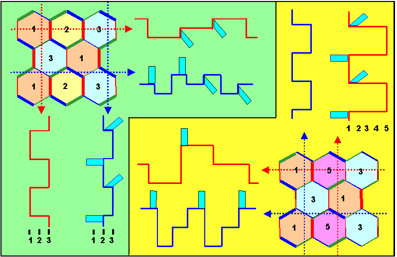
Shown are two possible combinations
of dislocations and steps in Σ = 3 boundaries
(of any kind). Dislocations in combination with a coherent step are indicated
in bold lines; the numbers in the hexagons indicate the level of the
boundary |
|
|
Two possible geometries are shown in the upper left-hand
corner and the lower right-hand corner |
|
|
Four cross-section through the dislocation/step network are
drawn in together with their schematic image in HRTEM. Ending lattice
fringes are indicated in light blue (assuming without justification that the
image of dislocation/step combinations that are inclined with respect to the
electron beam add no further complications). |
|
It becomes clear that the
interpretation of an HRTEM image can be a demanding task which will not
necessarily give an unambiguous answer. You may try your skills at the
picture in the
illustration. |
|
But we are still not done with the
discussion of the intrinsic geometry of a simple Σ = 3 boundary. Even if we assume that we have a
dislocation/step network of a defined kind (e.g. the one from the upper
left-hand corner of the above drawing) and that the boundary is flat apart from
the ups and downs of the dislocations, we must expect an added complication: |
|
|
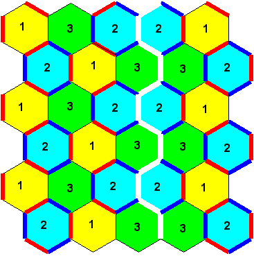
Since the dislocations/step network most likely formed in
small patches and then spreads out, individual patches may be out of
"synch", i.e. whenever they meet they will not fit together. This is
illustrated below |
|
|
|
|
|
|
|
|
Dislocations in combination with a coherent step are shown in
bold; the color now denotes if the step goes up or down as seen from the inside
of the hexagons completely enclosed by "bold" dislocations. The
dislocations/step network on the left and right side are identical, but
displaced relative to each other by one hexagon. |
|
|
Along the white line, they obviously don't match. We would
need dislocations with a step height of zero, which as we have seen before,
do not exist in this geometry. |
|
The only way out is to postulate a
new kind of defect, some kind of stacking fault in the dislocation/step
lattice. To the best of my knowledge, such a defect has not yet be named or
discussed in detail - although it is clearly a necessary feature of general
phase- or grain-boundaries. |
|
|
This serves to illustrate that the last word
about structural aspects of defects in crystal has not yet come in. One may
ask, of course, if esoterica like the dislocation/step network considerations
are of any importance. The answer is: Who
knows? |
|
|
Considering however, that many materials
(including natural minerals) are full of phase and grain boundaries, that many
properties of theses boundaries are directly linked to their structure and that
not much is known about the atomic structure of non-trivial boundaries, it is
not totally unrealistic to expect that research will go on. |
|
In the next (and last)
subchapter we will briefly look at some more questions in relation to phase
boundaries. |
© H. Föll